
Heat transport physics at micro/nanoscale |
|
 |
|
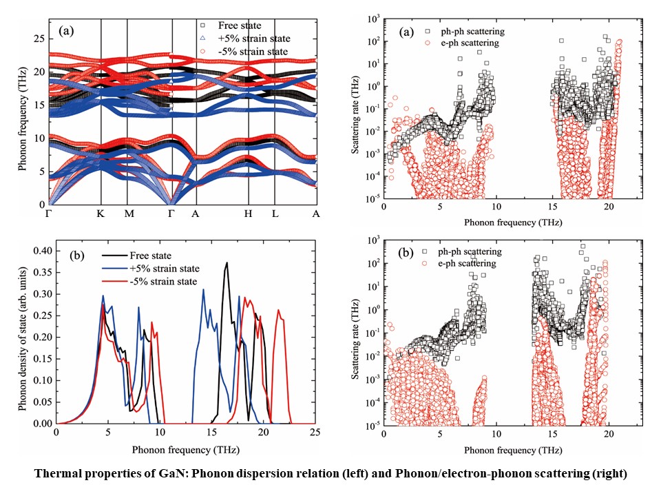
At normal macroscale, heat transports in a diffusive way, namely random walks of heat carriers under frequent internal scattering, and heat transport can be characterized by the classical Fourier’s law of heat conduction. At micro/nanoscale, however, the system size becomes comparable to the mean free path or the wave length of heat carriers (i.e. phonons in semiconductors), where heat transports in a non-diffusive way and the Fourier’s law breaks down. The microscopic details of heat carriers, such as energy spectrum, dispersion relation, frequency dependence, will play a dominant role in micro/nanoscale heat transport. Much attention should be paid to ballistic effects from the decreased internal scattering compared to boundary scattering, local non-equilibrium among different branches of phonons or electrons, localization near surfaces/interfaces, hydrodynamics by normal scattering, interface and geometry effects etc. The constitutive relation bridging heat flux and temperature field would benefit from the phonon Boltzmann transport equation using Boltzmann or Planck distribution and the fractional-order transport theory based on Levi walks. |
|
Thermophysical properties of micro/nanostructures-Numerical simulations |
|
 |
|
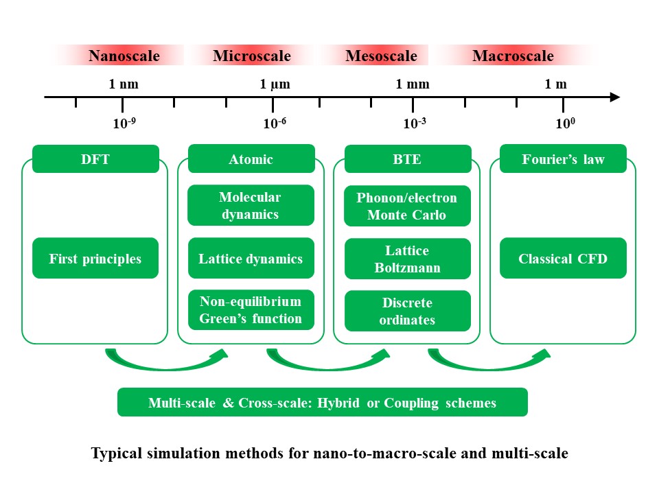
Due to the distinct physics of heat transport in micro/nanostructures from macroscopic understandings, computational methods are highly required to interpret underlying mechanisms, to predict novel phenomena, to assist experimental investigations, to design new nanomaterials, and to support engineering like transistors and thermoelectronics. The state-of-the-art computational approaches used in HEG include first principles based on solving Schrodinger equation, molecular dynamics tracking the evolution of atomic motions, lattice dynamics dealing with normal modes, non-equilibrium Green’s function calculating phonon transmission coefficient at interfaces, phonon/electron Monte Carlo numerically solving the Boltzmann transport equation. Different methods can be adopted to handle heat conduction problems at different range of scales from nanometer to meter mainly depending on the computation cost. The hybrid method and coupling scheme for multiscale heat transport are demanded in engineering problems. The most-recently-developed machine learning shows significant potential for data-driven studies of thermophyscial properties and speeding up the discovery of novel thermal materials. |
|
Thermophysical properties of micro/nanostructures-Experimental measurements |
|
 |
|
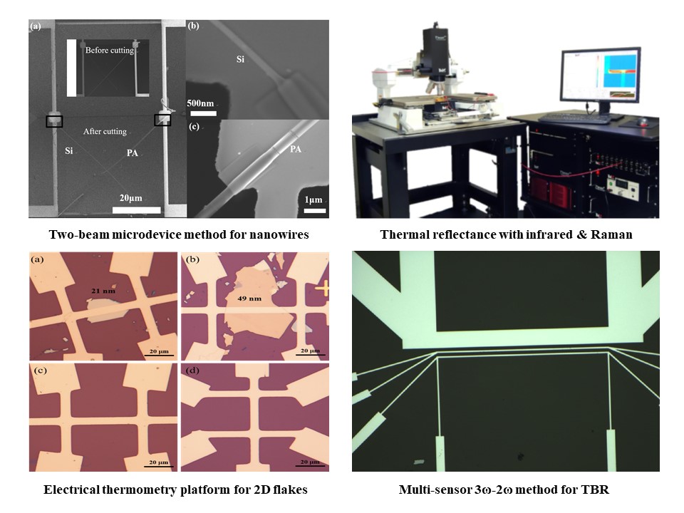
Experimental measurements for thermophysical properties of micro/nanostructures are extremely important but have great difficulty and uncertainty because of the special principles of experimental systems, the complex high-technology sample preparation, and the limit understanding of underlying physics etc. Future requirements point to high accuracy, wide scale range, non-destruction, in-situation and multi-parameters. Several typical techniques have been developed for micro/nanoscale thermal measurements, and HEG is focused those on IC-related semiconductor nanomaterials. The measurement technologies in HEG include the thermal reflectance system with infrared and Raman for ~100 nm resolution hotspots, the two-beam microdevice system for nanowires and fibers, the 3ω technique for micro/nano-films, the multi-sensor 3ω-2ω scheme for thermal interface resistance between films, the electrical thermometry platform for thermal and thermoelectrical properties of 2D flakes, and the laser flash system for bulk matters as benchmarks etc. |
|
Thermal managements and reliability of transistors and IC |
|
 |
|
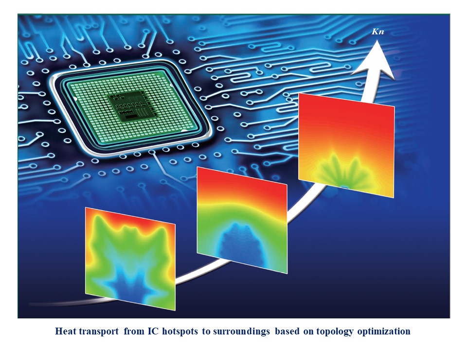
Heat dissipation dominates the reliability of IC and leads to over 50% of damages. Heat removal of modern transistors is stepping in more and more complicated situations, like ultra-wide bandgap semiconductors, smaller channel width, multi-dies and 3D packaging etc. First, huge and accurate database of thermophysical properties of micro/nanoscale semiconductors and their interfaces is highly desired. Second, the entire path, from heat generation, to heat transport and finally entering surroundings, covers multiple heat carriers, semiconductors and interfaces, in which hybrid and coupling simulations will be needed. Third, the temperature and stress inside transistors remain very difficult to be detected with enough resolution, especially in-situation and synchronization. Then, optimal design scheme has been very limited, and topology optimization with extensive freedoms becomes a candidate tool by considering thermal, electrical and mechanical issues. Future transistors will feature low energy cost and high heat conductance, which should challenge novel materials, physics and constructions. |
|
Thermal functional materials and thermal management devices |
|
 |
|
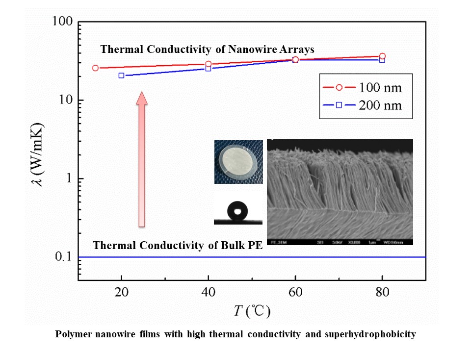
Materials are always a core problem for thermal managements of electronic devices. HEG is focused on semiconductors and nanocomposites with high thermal conductivity and low interfacial thermal resistance, and thermal smart materials with tunable thermal conductivity. Modern micro/nano-electronics are made of novel semiconductors with excellent thermal performance and buffer layers as heat bridges, like GaN, Ca2O3, SiC, AlN etc. Nanocomposites as thermal interfacial materials with both high thermal conductance and long lifetime are so significant for micro/nano-electronic devices that they must generally take into account different factors, including nanofillers, alignment/orientation, percolation, networking, surface chemical modification etc. Thermal smart materials with tunable thermal conductivity can be realized by controlling the internal structures, such as nanoparticle orientation of suspensions and polycrystalline degree of amorphous matters, on the basis of their external field dependence, among which electrical and temperature fields are preferred. Thermal management devices, like thermal rectifier and thermal rheostat, can be further developed. |
|
Microchannel cooling technologies for liquid-cooled chips |
|
 |
|
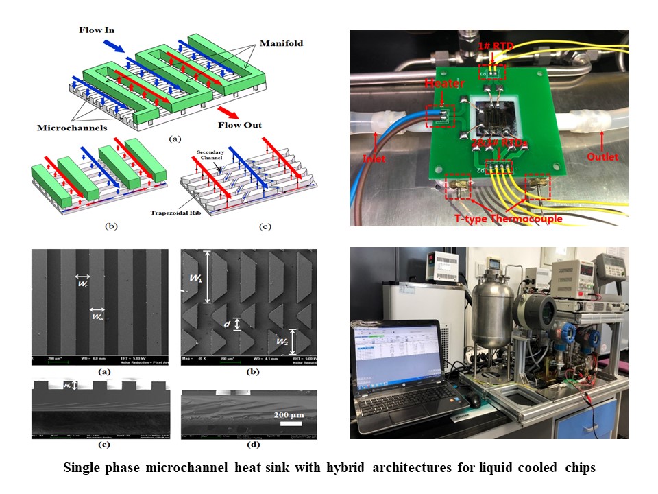
The heat flux in electronic devices keeps increasing because of the growing number of transistors in a chip and the 3D packaging technologies, which demands efficient cooling strategies to ensure the reliability and lifetime. Liquid cooling must be taken for heat dissipation density over ~100 W/cm2, noting it has been over 1000 W/cm2 in 5G and lasers. Microchannel cooling for inter-chip and intra-chip enhancements just meets the practical demands thanks to its excellent heat removal capability and high reliability. The optimization design of microchannels is a typical multi-objective issue involving in lowering the flow drag, enhancing the heat transfer coefficient, and increasing the temperature uniformity etc. Great efforts in designing optimal architectures, such as manifold and secondary oblique, are searching for its heat removal limit. The all-semiconductor fabrications should be taken for integrating the microchannel heat sink into a chip. Following single-phase scheme, the phase change microchannel cooling technique with higher heat removal capability is stepping from laboratories into engineering. |
|